
ANSYS SIwave: PCB Signal Integrity and Power Integrity Simulation for High-Speed Digital Designs
High-speed digital designs operating above 1 GHz routinely encounter signal integrity (SI) and power integrity (PI) failures that are invisible to traditional schematic-level analysis. ANSYS SIwave is a purpose-built electromagnetic simulation tool that addresses these challenges directly on the PCB layout, enabling engineers to identify and resolve SI/PI issues before the first prototype is built.
What Is ANSYS SIwave?
SIwave is a full-wave electromagnetic field solver optimized for planar structures such as PCBs, IC packages, and multi-chip modules. Unlike general-purpose 3D EM solvers, SIwave uses a hybrid finite-element/integral-equation approach that is specifically tuned for the layered geometries found in PCB stackups. This makes it orders of magnitude faster than brute-force 3D solvers for board-level analysis while maintaining accuracy up to tens of gigahertz.
SIwave integrates directly with Cadence Allegro, Mentor PADS, Altium Designer, and other major EDA platforms via native import, allowing engineers to simulate the actual routed board rather than a simplified schematic approximation.
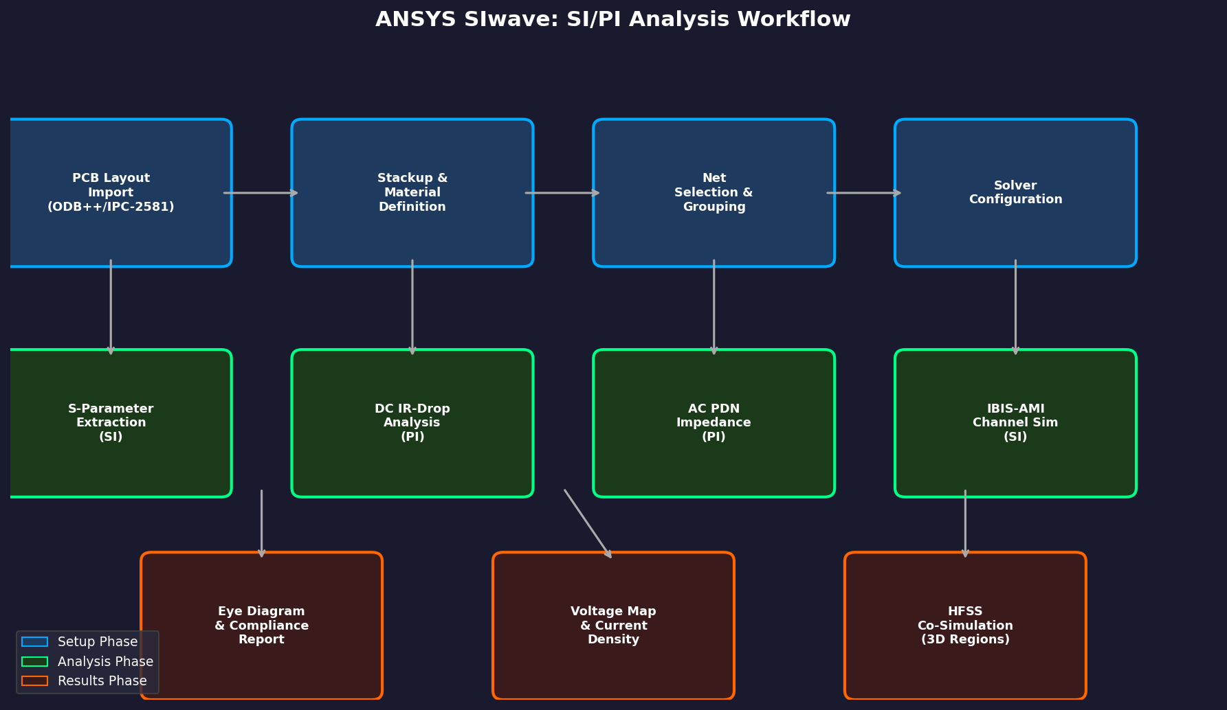
Signal Integrity Analysis Workflow
1. Importing the PCB Layout
SIwave reads ODB++, IPC-2581, or native EDA formats to reconstruct the full board geometry, including all copper layers, vias, differential pairs, and component footprints. The import process automatically identifies nets and assigns them to SI or PI analysis groups.
2. S-Parameter Extraction for Interconnects
The core SI workflow extracts S-parameters for critical nets — DDR5 data buses, PCIe lanes, USB 3.x differential pairs, and high-speed SerDes links. SIwave's solver computes frequency-domain S-parameters from DC to the user-defined maximum frequency (typically 2–5× the Nyquist frequency of the data rate). These S-parameters can then be exported as Touchstone (.snp) files for use in SPICE or system-level channel simulators such as ANSYS HFSS-SIwave co-simulation or Keysight ADS.
Key parameters extracted:
- Insertion loss (IL) and return loss (RL) per channel
- Near-end and far-end crosstalk (NEXT/FEXT) between adjacent traces
- Differential-to-common mode conversion (SCD21) for differential pairs
- Via stub resonances and their impact on channel bandwidth
3. Eye Diagram and Channel Compliance
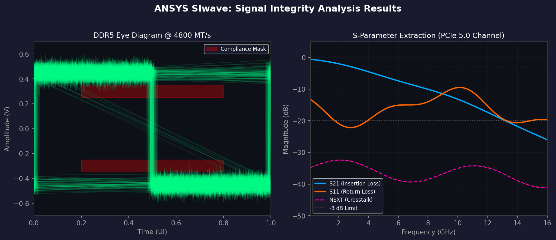
SIwave includes a built-in IBIS-AMI channel simulator. After extracting the interconnect S-parameters, engineers attach IBIS-AMI models for the transmitter and receiver, then run a statistical eye diagram simulation. The tool reports eye height, eye width, and bathtub curves against industry compliance masks (JEDEC DDR5, PCIe 5.0/6.0, USB4). This closed-loop workflow — from layout geometry to compliance report — can be completed in under an hour for a typical DDR5 memory channel.
Power Integrity Analysis
DC IR-Drop Analysis
SIwave's DC solver computes resistive voltage drop across the power delivery network (PDN) for each power rail. The result is a color-coded voltage map overlaid on the PCB layout, immediately revealing areas where copper pour resistance or via current density exceeds design margins. Engineers can interactively adjust plane shapes, add vias, or increase copper weight and re-run the DC analysis in seconds.
AC Impedance and PDN Resonance
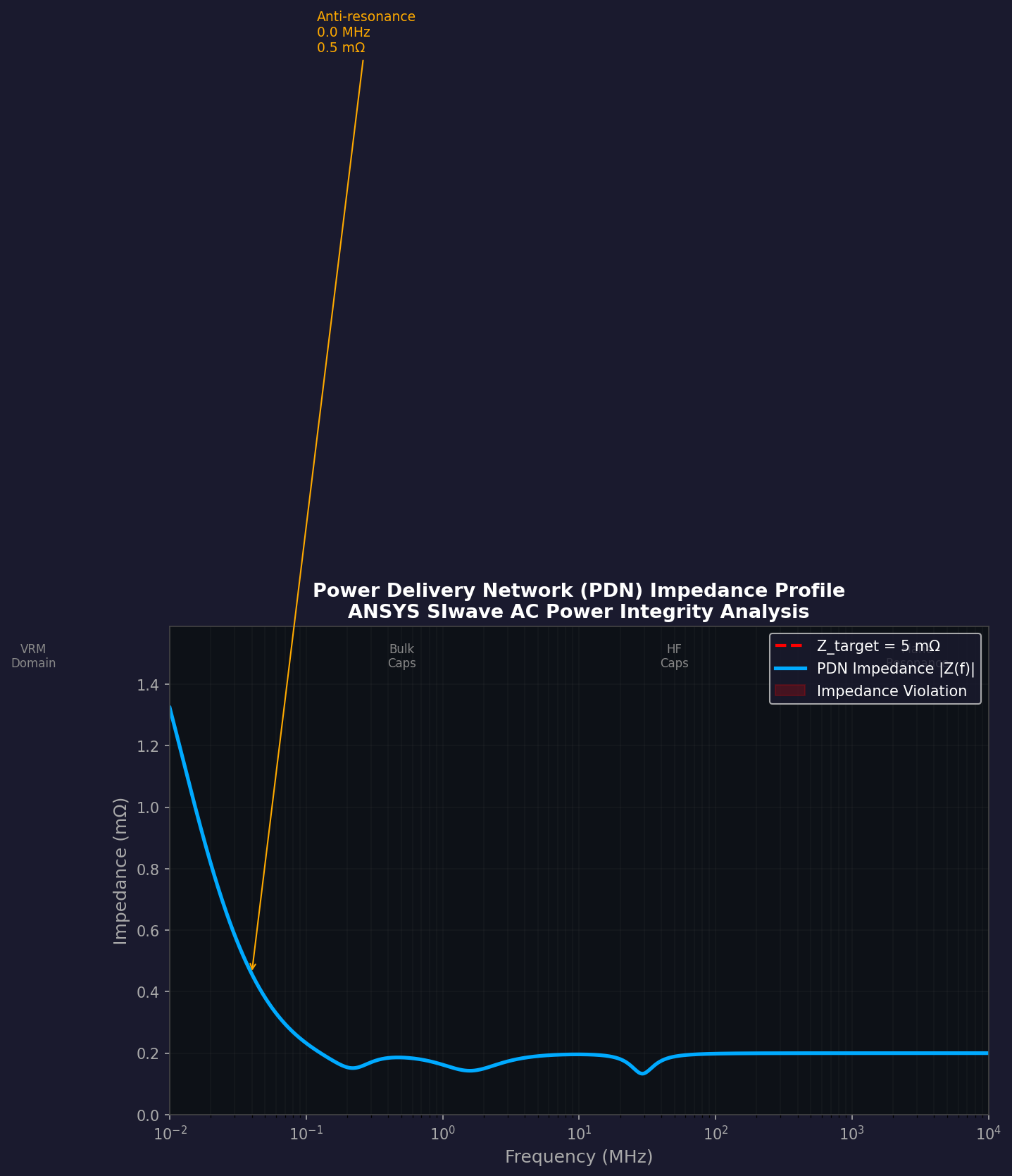
The AC PI workflow computes the PDN impedance spectrum (Z-parameter) from the voltage regulator module (VRM) output to the IC power pins. SIwave models the VRM as a frequency-dependent impedance source and includes all decoupling capacitors with their parasitic inductance (ESL) and resistance (ESR) extracted from component models or S-parameter measurements.
The resulting impedance plot reveals:
- Anti-resonance peaks where PDN impedance exceeds the target impedance (Z_target = ΔV / I_transient)
- Frequency ranges where decoupling capacitor placement is ineffective due to via inductance
- Plane resonances that can couple switching noise into sensitive analog circuits
A well-designed PDN maintains impedance below Z_target from DC to the highest significant harmonic of the switching current — typically 5–10× the clock frequency.
Simultaneous Switching Noise (SSN)
When multiple I/O drivers switch simultaneously, the resulting current transients induce voltage fluctuations on the power and ground planes — a phenomenon known as simultaneous switching noise or ground bounce. SIwave's transient PI solver computes SSN by convolving the PDN impedance with the time-domain current waveforms from IBIS models, providing a direct estimate of supply voltage noise at each IC power pin.
Integration with ANSYS HFSS and Icepak
For designs where via transitions, connectors, or BGA escape routing require full 3D EM accuracy, SIwave supports seamless co-simulation with ANSYS HFSS. The engineer defines a 3D region of interest within SIwave, and HFSS automatically meshes and solves that region, with the results fed back into the SIwave board-level model. This hybrid approach delivers 3D accuracy where needed without the computational cost of solving the entire board in 3D.
SIwave also links to ANSYS Icepak for thermal-aware PI analysis, accounting for the temperature dependence of copper resistivity in high-current power planes.
Best Practices for SIwave Simulations
- Validate the stackup first. Accurate dielectric constants (Dk) and loss tangents (Df) are critical above 5 GHz. Use measured values from the PCB fabricator's material datasheet, not nominal values.
- Set the frequency sweep range appropriately. For a 32 Gbps SerDes link, simulate to at least 32 GHz (the 5th harmonic of the fundamental). Undersampling the frequency range will miss via stub resonances.
- Include all decoupling capacitors. Missing even a few bulk capacitors can shift PDN resonance frequencies by hundreds of megahertz.
- Use IBIS-AMI models from silicon vendors. Generic IBIS models underestimate equalization effects and produce overly pessimistic eye diagrams.
- Correlate with measurements. Use a vector network analyzer (VNA) to measure S-parameters on a test coupon and compare with SIwave predictions. Discrepancies above 3 dB at the Nyquist frequency indicate a stackup or geometry modeling error.
Conclusion
ANSYS SIwave provides a comprehensive, layout-accurate environment for signal integrity and power integrity analysis of high-speed PCBs. By combining full-wave EM extraction, IBIS-AMI channel simulation, DC IR-drop, and AC PDN impedance analysis in a single tool, SIwave enables hardware engineers to close SI/PI margins analytically rather than empirically — reducing costly board respins and accelerating time to market.
Further Reading: