Keysight ADS Momentum: 3D Planar EM Simulation for High-Frequency PCB and RFIC Design
Introduction
As operating frequencies push into the millimeter-wave range, the gap between schematic-level circuit simulation and real-world hardware performance widens dramatically. Parasitic coupling, substrate modes, and radiation losses that are invisible at lower frequencies become dominant failure mechanisms above 5 GHz. Keysight Advanced Design System (ADS) Momentum is a 3D planar electromagnetic (EM) solver purpose-built to bridge this gap, enabling engineers to co-simulate passive structures—transmission lines, couplers, antennas, and package interconnects—alongside active circuit models within a single design environment.
This article examines the practical workflow for using ADS Momentum to characterize high-frequency PCB structures and RF integrated circuits (RFICs), with a focus on the setup choices that most directly affect accuracy and simulation throughput.
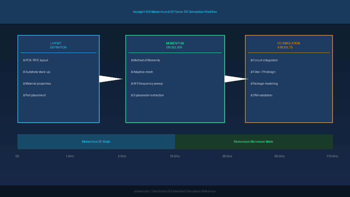
What Is ADS Momentum?
ADS Momentum is a Method-of-Moments (MoM) EM solver integrated natively into the Keysight ADS schematic and layout environment. Unlike full 3D finite-element tools (e.g., ANSYS HFSS), Momentum operates on stratified planar media: it assumes that conductors lie in one or more horizontal layers embedded in a stack of dielectric sheets. This assumption is valid for the vast majority of PCB, LTCC, and RFIC structures, and it allows Momentum to reduce a 3D problem to a 2D surface integral—delivering results orders of magnitude faster than volumetric solvers for the same class of geometry.

Two solver modes are available:
| Mode | Best For | Frequency Range |
|---|---|---|
| Momentum RF | Microwave circuits, filters, couplers | DC – ~30 GHz |
| Momentum Microwave | Millimeter-wave, antenna arrays, package interconnects | 10 GHz – 110 GHz+ |
Momentum Microwave adds full-wave radiation modeling and is required whenever the structure's electrical size approaches a wavelength.
Substrate Stack-Up: The Foundation of Accuracy
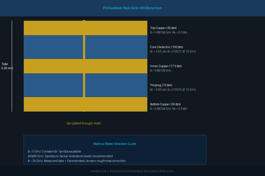
The single most impactful setup decision in any planar EM simulation is the substrate definition. Momentum requires:
- Layer thicknesses for each dielectric and metal layer
- Relative permittivity (εr) and loss tangent (tan δ) for each dielectric
- Conductivity (σ) and surface roughness for each metal layer
For standard FR-4 at 2.4 GHz, nominal datasheet values (εr ≈ 4.3, tan δ ≈ 0.02) are adequate. At 28 GHz or above, however, the frequency-dependent behavior of εr and tan δ must be captured using a Djordjevic-Sarkar or Wideband Debye material model. Keysight provides built-in material libraries for common laminates (Rogers RO4003C, Isola I-Tera MT40, etc.), and custom entries can be imported from vendor-supplied Touchstone or CSV files.
Surface roughness is equally critical at millimeter-wave frequencies. The Hammerstad-Jensen roughness model, accessible in the substrate editor, applies a frequency-dependent correction factor to conductor loss that can increase insertion loss predictions by 1–2 dB/cm at 60 GHz on standard electrodeposited copper.
Mesh Control and Convergence
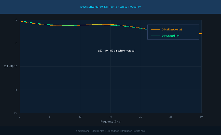
Momentum uses an adaptive mesh that subdivides conductors into rectangular and triangular cells. The default edge mesh setting places finer cells near conductor edges where current density peaks—this is essential for accurate loss modeling in narrow microstrip lines and coplanar waveguide (CPW) structures.
Key mesh parameters to tune:
- Cells per wavelength: Default is 20; increase to 30–40 for structures with tight coupling or sharp bends.
- Edge mesh width: Set to approximately 10–20% of the conductor width for microstrip, or the gap width for CPW.
- Thick metal modeling: Enable for conductors thicker than 3 µm (relevant for RFIC top-metal layers) to capture current redistribution through the conductor cross-section.
A practical convergence check is to run the simulation at two mesh densities (e.g., 20 and 30 cells/wavelength) and compare S-parameters. If |ΔS21| < 0.1 dB and |ΔS11| < 0.5 dB across the band, the coarser mesh is sufficient.
Co-Simulation with Circuit Models
One of Momentum's most powerful features is EM-circuit co-simulation, which allows the S-parameter block generated by Momentum to be instantiated directly in an ADS schematic alongside transistor models, lumped components, and behavioral blocks. This workflow is essential for:
- Filter design: Simulate the EM response of the resonator structure, then tune lumped coupling elements in the schematic to meet the passband specification.
- Power amplifier matching networks: Replace ideal transmission-line models with Momentum-extracted S-parameters to capture substrate coupling and via inductance.
- Package modeling: Import a Momentum simulation of the bond-wire or flip-chip bump array and co-simulate with the die model to predict package resonances before tape-out.
The co-simulation link is bidirectional: changes to the layout automatically re-trigger the EM simulation when the schematic is swept, ensuring that the circuit and EM domains remain synchronized throughout the design iteration.
Practical Tips for Efficient Simulation
-
Use port de-embedding aggressively. Momentum's internal ports eliminate the need to extend feed lines to the substrate boundary, reducing mesh size and simulation time by 30–50% for compact structures.
-
Leverage the Adaptive Frequency Sampling (AFS) engine. Rather than simulating at every frequency point, AFS fits a rational function to a sparse set of computed points and interpolates. For a 100-point sweep from 1–40 GHz, AFS typically requires only 15–25 full EM solves.
-
Partition large layouts. For a full PCB with multiple RF sections, simulate each functional block (filter, balun, coupler) independently and assemble the S-parameter blocks in the schematic. This reduces peak memory usage and enables parallel simulation on a compute cluster.
-
Validate against measurement early. Fabricate a simple test coupon—a 50 Ω microstrip through-line and a coupled-line section—and compare Momentum predictions against VNA measurements before committing to a full-board simulation. Discrepancies larger than 0.5 dB/cm in insertion loss typically indicate a substrate parameter error.
Conclusion
ADS Momentum occupies a well-defined niche in the RF/microwave design flow: it is fast enough for iterative design exploration yet accurate enough to replace physical prototypes for most planar passive structures. Mastering the substrate stack-up definition, mesh convergence workflow, and EM-circuit co-simulation link transforms Momentum from a verification afterthought into a first-principles design tool that catches layout-induced performance degradation before a single board is fabricated.
For engineers working above 10 GHz, integrating Momentum into the early design phase—rather than as a final sign-off step—is one of the highest-leverage practices available in modern RF design.